Measuring microstructures, testing microtechnology
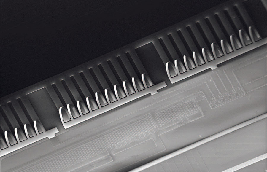
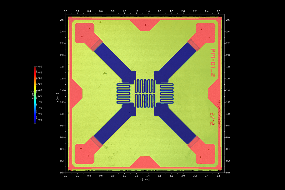
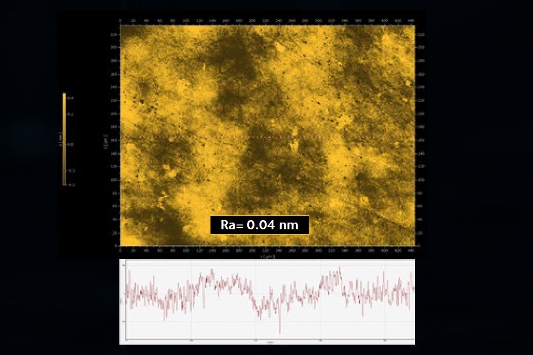
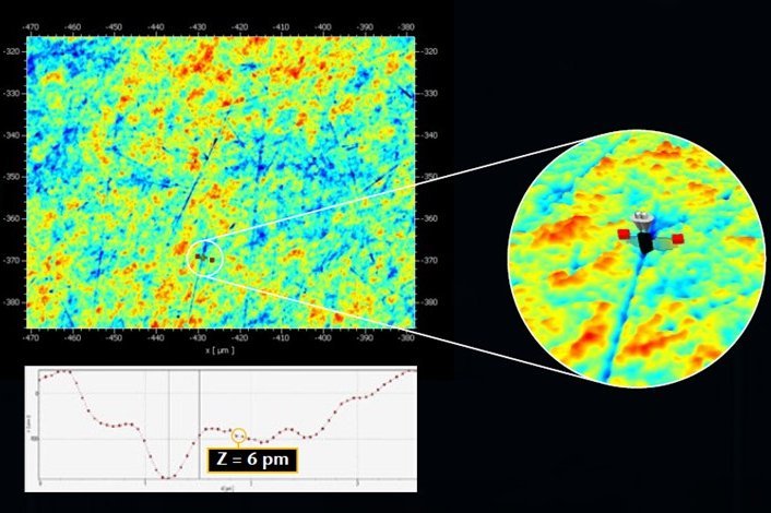
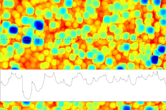
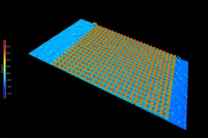
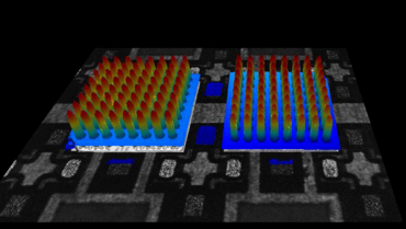
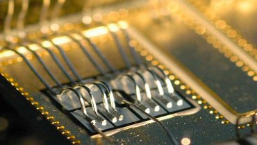
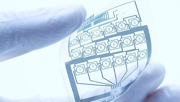
Miniaturizing functional components enables numerous applications and innovations, whether in consumer electronics, automotive, wearables or medical technology. Micro-electromechanical systems (MEMS) or microoptics place high demands regarding sophisticated testing, presenting new challenges to respective measurement technology and testing tools. Complex microstructures require a comprehensive analysis, ideally including areal inspection with high resolution (µm to nm range), revealing insights regarding quality and functionality.
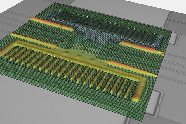
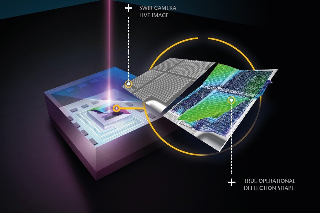
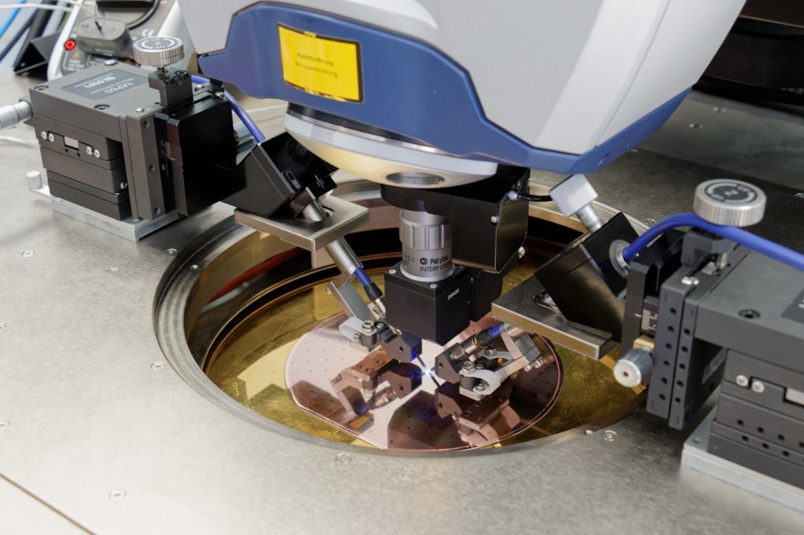
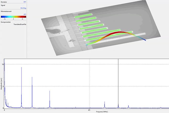
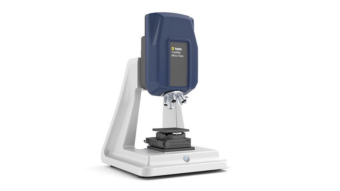
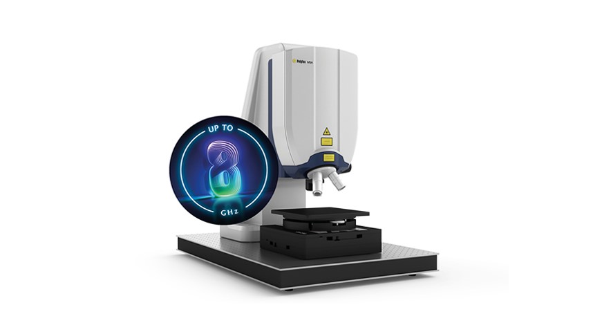
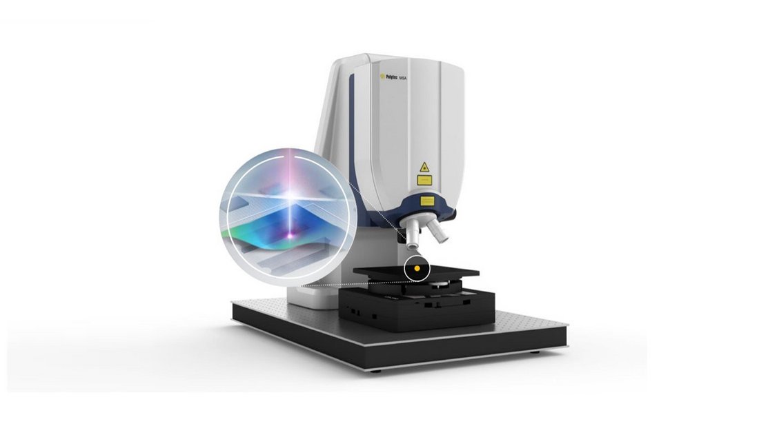
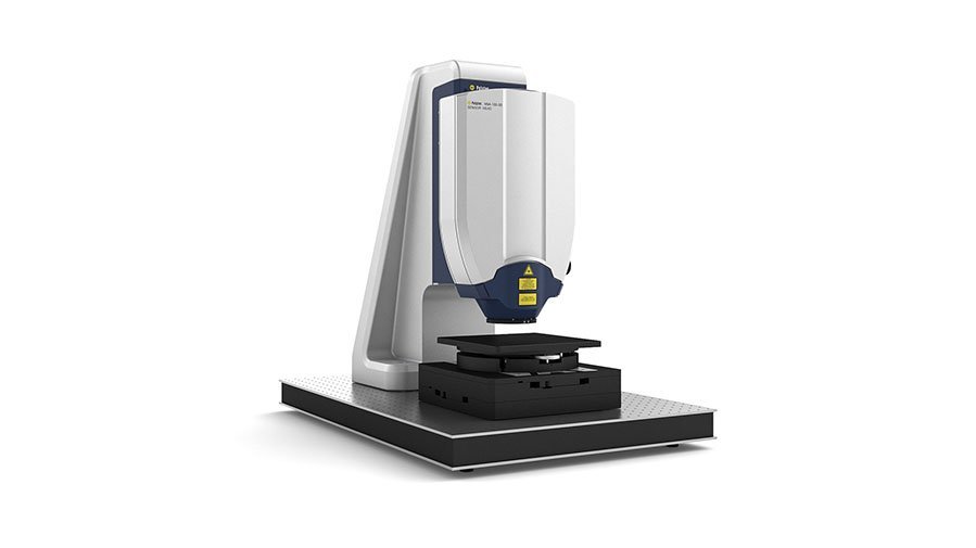
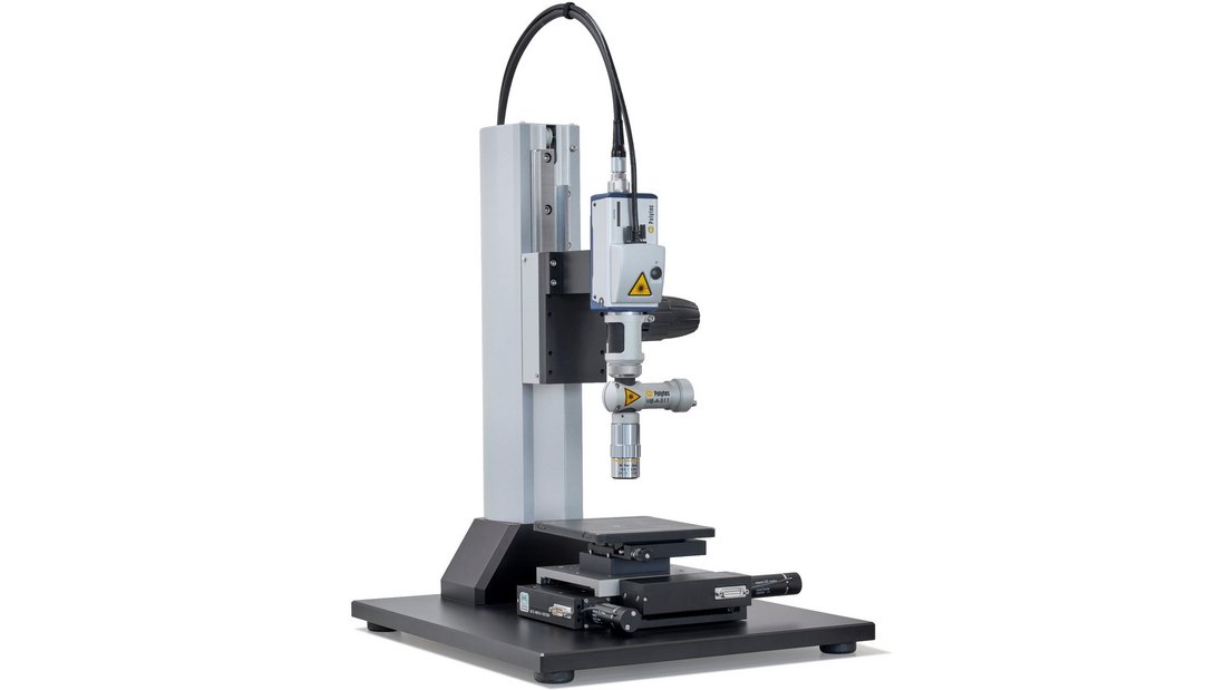
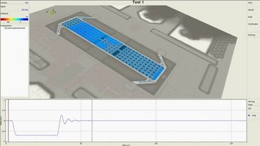
Polytec optical measurement solutions allow characterizing both the areal topography, form and structural details as well as testing the dynamic motion and behaviour of MEMS and microsystems.
How do you inspect topography, finish or microstructures?
We measure your MEMS and microstructures and analyze them with you!

Tactile vs optical measurement of microstructures
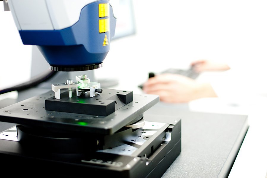
Tactile surface measurement technologies face limits when it comes to microstructure analysis since the complex structural details are difficult to be transferred over an entire surface using a 2D profile line or it can become quite time-consuming. A reference line is used here, often referred to as roughness profile, often becoming the basis for further evaluation. Tactile measurements with stylus tips can leave marks on the surface and are subject to wear, which can affect repeatability over time. A non-invasive optical testing method shows particular advantages for precision surfaces in mechanical engineering, offers reproducible measurements, does not lead to NOK parts and proves to be faster and more cost-effective for full-areal measurements or 100% inspections in production or research.
We measure your samples and show what's possible in free feasibility studies!
